


Temperature influences electronic component behavior and characteristics in numerous ways. The effects are not limited to the components that get hot directly, but also those that are indirectly affected — for example, due to proximity or the PCB material’s thermal properties. Thus, PCB designers must account for the component’s and PCB’s thermal properties to ensure safe, reliable, and error-free operation throughout the device’s entire lifetime. Heat sink dimensioning and placement, the right choice of PCB materials, and adequate traces and thermal relief vias all influence heat dissipation and ensure adherence to safety standards and the product’s reliability.
The Concept of Thermal Resistance
Thermal resistance as a concept is vital in PCB thermal management: it quantifies how effectively a material can conduct or convect heat. Like electrical resistance, thermal resistance refers to how a material hinders heat flow, and lower thermal resistance values suggest better heat dissipation capabilities.
Thermal resistance accounts for two main modes of heat transfer: conduction and convection. In this model, the heat transfer rate (q) follows a concept similar to the electrical charge transfer rate (I) described by Ohm’s law; however, a temperature differential acts as the driving force instead of voltage.
Conduction describes heat transfer through a material by molecular interaction. In PCBs, this typically occurs through the substrate, conductive traces, and heat sinks. The heat generated by an electronic component conducts through the materials surrounding it due to the temperature differential between the contacting materials. Convection involves the heat transfer through a fluid medium, such as air or liquid. As components warm up, they transfer heat to the surrounding air, which is colder than the components.
The two modes of heat transfer co-occur, and the ambient temperature influences the driving force. PCB designers can often neglect the thermal mass of components and the circuit board unless working on high-power or high-pulse current applications. The thermal mass refers to a material’s ability to store heat. Materials with higher thermal mass can absorb and retain more heat energy before their temperature rises, while materials with lower thermal mass heat up and cool down more quickly.
Heat’s Impact on Electronic Components and PCBs
Managing the heat generated by electronic components is essential to ensuring a circuit’s optimal performance and reliability. As temperatures rise, electronic components and the traces on the PCB experience changes in their electrical properties. For example, resistance increases in resistors and traces with rising temperatures, and capacitors can exhibit similar changes in capacitance. Prolonged thermal stress can also degrade the component’s materials, eventually leading to failures. More complicated microcontrollers and microprocessors often throttle their performance with inadequate thermal dissipation, leading to suboptimal functioning.
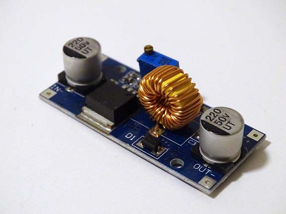
Soldering a heat-generating component’s heat sinks to the PCB helps spread the dissipated thermal energy to the entire surface by reducing the thermal resistance.
In the PCB itself, excessive heat can contribute to changes in signal integrity, noise generation, and signal distortion. Designers must pay close attention to the thickness, height, and positioning of traces and vias that carry high currents because their resistance accounts for significant losses and, thus, heat generation.
Thermal cycling and prolonged heat stress also affect solder joints, which expand and contract based on the board’s temperature. Insufficient cooling can affect solder joints over extended periods and lead to mechanical failure.
The Context’s Impact on Heat Dissipation
As the temperature difference is the main driving force of heat dissipation in the thermal resistance model, designers must consider the PCB’s target use case and environment. Thus, designs that will be used in high-temperature environments dictate different design requirements compared to ones that operate in colder climates. Additionally, a circuit’s operation altitude similarly affects heat dissipation, which is especially relevant in aviation and military applications.
PCBs for specific contexts, such as manufacturing, aviation, or military applications, must resist different thermal stresses than consumer devices. In addition to environmental requirements, designers should ensure adherence to industry standards such as IPC-2152 and IPC-2221. Moreover, additional government regulations may be in place in some domains.
Component Placement Considerations
PCB designers must identify potential thermal hot spots to ensure adequate heat dissipation. These are typically caused by electronic devices such as highly integrated circuits that generate significant thermal losses. Similarly, high-current devices like power MOSFETs and high-current traces often emit large amounts of thermal energy.
Spacing such components and traces adequately far apart on the board mitigates the formation of hot spots and spreads the heat evenly across the entire PCB surface. The hottest components should be placed in the center of the board to maximize the area for the heat to spread.
If designers can choose between different package sizes for the same component, picking larger package sizes can help increase the thermal contact area of devices with the board. Similarly, thicker and wider traces can help dissipate more heat, especially in high-power applications.
Solder Pad Size Considerations
Naturally, thicker mounting pads can also dissipate more heat away from the connected component to the surrounding board material. Designers can tweak the top layer’s pad thickness to balance the circuit’s thermal properties. However, they must do so in accordance with the trace’s signal integrity requirements, as the pad thickness affects impedance, which might be problematic in controlled impedance designs when not accounted for.
How Thermal Vias Facilitate Effective Heat Dissipation
Depending on the type, thermal vias provide a heat transfer path from one side of the PCB to the center of the board or the other side. Due to their conductive properties, thermal vias act as heat pipes that help spread heat from one side of the board across the entire PCB’s surface and stackup.
These thermal vias should be placed in a regular pattern near the surface-mounted, heat-generating component’s thermal solder pad. The vias should be exposed to the side that houses the heat-generating component to reduce thermal resistance. However, on the opposite side, the via should be covered by the solder mask to prevent the solder from flowing to the wrong side of the board during assembly.
Thermal vias help spread the heat to large planes situated on the underside of the PCB.
When connected to a GND plane, thermal relief vias can provide excellent low-impedance return current paths for devices. As with other large planes, designers should consider placing thermal relief patterns around solder points to facilitate easy soldering. To further optimize the solder process, designers can have the vias filled with epoxy or capped with copper to prevent uncontrolled solder flow. However, they must remember the current requirements to prevent thermal relief patterns from acting as fuses unintentionally.
Conclusion
Managing heat in PCB design is crucial for optimal performance and reliability. Thermal hot spots, often from highly integrated circuits or high-current devices, require attention to prevent localized heating.
Adequate spacing and positioning of components help spread heat evenly across the PCB. Carefully balancing mounting pad size and trace thickness ensures sufficient cooling while aligning with signal integrity requirements.
Thermal vias act as heat pipes, transferring heat from one side of the PCB to the other, and should be strategically placed near heat sources. Exposed vias on the component side reduce thermal resistance, while covered vias prevent solder flow issues during assembly. Designers may choose to fill vias with epoxy or cap them with copper for controlled soldering.
