


After formalizing a circuit’s functionality in a schematic diagram and deciding on the parts, devices, and technologies to employ, the next step is to create a functional PCB layout. This step aims to place all components on the PCB and establish all necessary connections, ensuring that the board dimensions are minimal and that application-specific goals, such as minimal losses or maximal signal integrity, are met. However, the process can be intricate and involves more than merely drawing connections between electronic components. This article covers vital best-practice approaches to keep in mind during this crucial phase in a product’s lifecycle.
Leverage Subcircuits for Optimal Component Placement
Subcircuit identification in PCB design significantly influences device placement and routing strategies. By isolating specific functional blocks within the circuit, designers can strategically position components to ensure efficient utilization of PCB space and short signal pathways, minimizing crosstalk and the potential for signal decay. This process directly impacts device placement, and sensitive low-voltage areas should be strategically positioned away from high-voltage sections to prevent signal corruption and ensure safe and reliable operation.
Engineers must also account for the space required by decoupling capacitors and vias in designs containing digital ICs to ensure a reliable supply during brief demand peaks. Additional vias between decoupling capacitors and the power pins can help increase the capacitance by leveraging the plane capacitances.
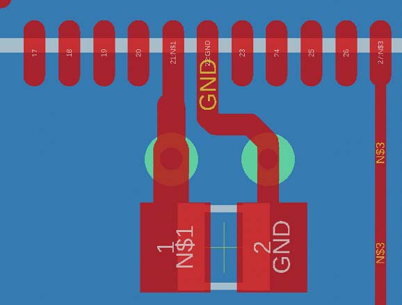
This image illustrates how the left trace gets thinner as it merges into the IC pin. The figure also depicts how vias can be placed between a decoupling capacitor and the supply pins.
Thermal management can also influence the placement of individual components or entire sub-circuits. Components sensitive to heat can exhibit different characteristics and should be placed away from parts that produce heat, particularly if the PCB is used as a heat sink. Designers should account for the space and clearance requirements of external heat sinks.
Routing: More Than Just Placing Wires
The traces require significant space on a PCB, and various manufacturing constraints and the physical and electrical characteristics of the conductive material influence routing. When done correctly, PCB design engineers can ensure reliable operation while minimizing the necessary board space.
Engineers should try to minimize trace lengths, even on non-critical designs that don’t require precise impedance or signal path matching. Signals decay the farther they have to travel. Longer traces exhibit higher resistance, leading to signal attenuation and weakening — in turn, making the circuit more susceptible to noise. Similarly, longer traces have a more significant potential of introducing electromagnetic inference and signal decay. They can act as antennas and pick up or radiate EMI, influencing nearby sensitive components.
Trace width also contributes to a circuit’s impedance and susceptibility to electric noise. As thick traces are more sensitive to noise, engineers should strive to minimize trace widths whenever possible. However, they must ensure that traces meet the current requirements, especially when they carry power. In RF and high-frequency applications, thick traces should gradually get thinner toward the pads to maintain signal integrity and help minimize signal reflection. Signal-carrying traces should not run parallel over long distances to reduce signal crosstalk between the traces. Similarly, too narrow spacing between traces can increase cross-coupling, so engineers should strive to separate the traces by at least three times the dielectric thickness.
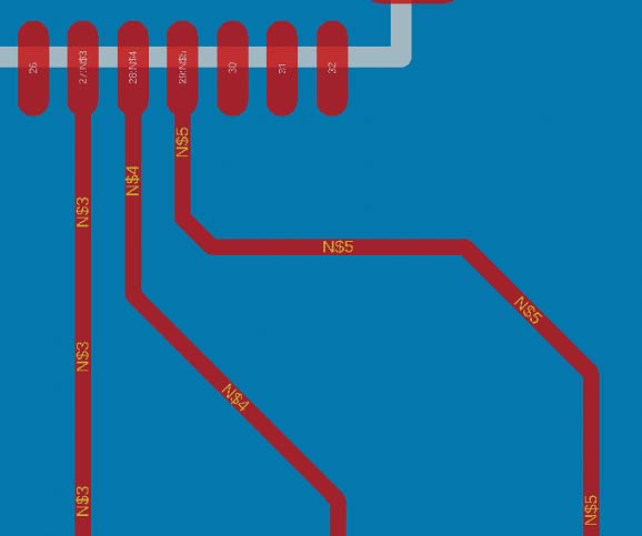
Routing signal wires farther apart instead of in parallel can prevent crosstalk between susceptible signals.
Finally, vias should always be placed in pairs and designers should always put a GND via as close as possible to signal and power vias to improve via inductance and enhance current return paths — minimizing signal distortion and crosstalk.
Perform Layer Stackup Optimization on Multi-Layer PCBs
Traces on one layer don’t exist in isolation from the others, and they are affected by traces and pads on other layers if not routed with care. Solid reference and supply planes influence the capacitance and signal integrity of other traces on the PCB. Engineers should ensure signal and power traces run above a solid reference plane. Typically the reference is 0V, but it can also be another suitable power plane in some instances. The reference plane should not have significant gaps. If it does, signal traces should not run over the gaps to avoid critical EMI problems in susceptible applications.
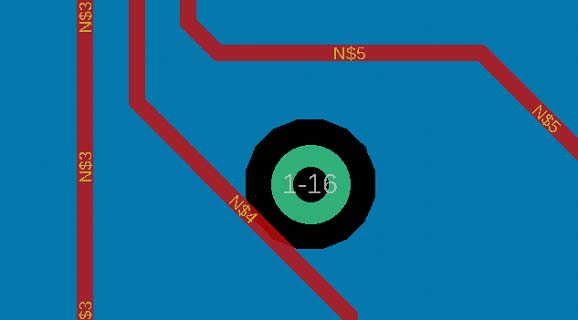
Vias placed close to traces can prevent the affected trace from running over an underlying solid copper layer.
Placing vias can, for example, create gaps in planes when the via is not connected to the reference plane. When placed too closely to a signal trace, the via can create a gap in the reference plane and leave the signal trace exposed.
Summary
Creating a functional PCB layout involves strategic component placement and efficient connection routing to meet application-specific goals. Subcircuit identification plays a crucial role, allowing designers to optimize space utilization, minimize signal decay, and prevent crosstalk. Thermal management considerations also influence component placement, particularly for heat-sensitive parts. Decoupling capacitors and vias are vital for reliable supply, and careful attention must be given to their placement in designs with digital ICs.
Efficient trace design is essential, considering the impact of manufacturing constraints and the conductive material’s characteristics. Engineers should minimize trace lengths to reduce signal decay and electromagnetic interference. Trace width influences impedance and noise susceptibility, necessitating a balance between width and current requirements. Careful consideration of vias, especially their pairing and proximity to signal traces, is crucial for minimizing signal distortion and crosstalk.
Multilayer PCB routing involves layer interactions, and solid reference planes affect capacitance and signal integrity. Ensuring signal and power traces run above a solid reference plane is crucial, avoiding gaps to prevent EMI issues. Vias, if improperly placed, can create gaps in reference planes. Ground and supply planes, along with decoupling capacitors, are effective in mitigating brownout issues during short current spikes.
