| PCB QUOTE |
[PDF] Download PCB Capabilities Sheet »
Microvias in Advanced PCB Designs
Advanced Circuits offers expanded PCB manufacturing capabilities including laser-drilled microvias for high-tech requirements. Microvias and stacked microvias can be found in High Density Interconnect circuit boards, also known as HDI PCBs, to enable complex interconnections in advanced designs.
Microvias, stacked microvias, and via-in-pad features allow miniaturization for higher functionality in less space and can accommodate large pin-count chips such as the ones used in cell phones and tablets. Microvias help reduce layer count in printed circuit board designs while enabling higher routing density and eliminating the need for through vias.
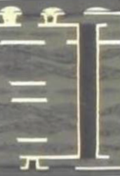
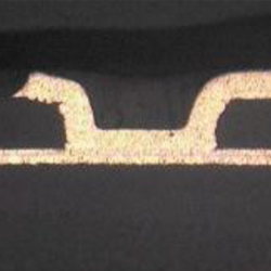
Standard Microvia PCB Microsection

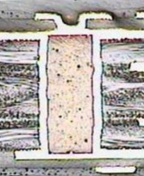
Microsections of Microvias Exhibiting Uniformity of Plating
No occlusions, voids, or skips
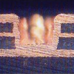
Copper-Filled Microvia Microsection
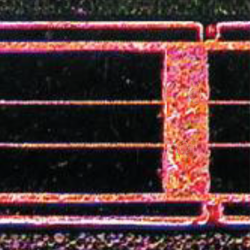
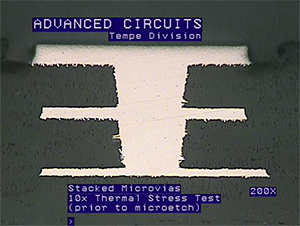
Stacked Microvia Microsection
Advanced Circuits Microvia Capabilities
Refer to the chart below for Advanced Circuit's HDI / Laser Drilled Microvia (μVia) Capabilities
| Smallest (as ablated) Laser Microvia | 0.003" |
| Largest (as ablated) Laser Via | 0.010" |
| Microvia Aspect Ratio (Depth to Diameter) |
0.75:1 Standar / 1:1 Advanced |
| Capture Pad Size | μVia +0.008" Std. / μVia +0.006" Adv. |
| Landing Pad Size | μVia +0.008" Std. / μVia +0.006" Adv. |
| Stacked Microvia | Yes |
| Type I Capabilities | Yes |
| Type II Capabilities | Yes |
| Type III Capabilities | Design Dependent |
| Copper Filled Microvias | Yes |
High-density interconnects are categorized by six design types in IPC-2226. They are grouped by stackup characteristics in the following categories: Type I, Type II, Type III, Type IV, Type V, and Type VI
- TYPE I 1 [C] 0 or 1 [C] 1, with through-vias from surface to surface.
- TYPE II 1 [C] 0 or 1 [C] 1, with buried vias in the core and may have through-vias connecting the outer layers from surface to surface.
- TYPE III 2 [C] 0, two or more HDI layers added to through-vias in the core or from surface to surface.
- TYPE IV 1[P] 0 where P is a passive substrate with no electrical connecting functions.
- TYPE V Coreless constructions using layer pairs.
- TYPE VI Alternate constructions of coreless construction using layer pairs.
For more information about Microvias and other advanced PCB capabilities, Click here to contact us or download our full capability sheet.
Capabilities for Advanced Requirements
- Microvia
- Stacked Microvias
- HDI Boards
- Multilayer RF & Microwave
- Heavy Copper
- Oversized Boards
- Laser Direct Imaging (LDI)
- Air Pockets Between Layers
- Buried Chip Resistors
- Via-in-Pad
- Learn more →