


Printed circuit boards (PCBs) form the vital backbone of practically all modern electronic devices, as they facilitate the production of intricate yet reliable designs in large quantities. By providing stable mounting points for electronic components and reliably connecting them, PCBs enable higher levels of integration, increase the overall reliability of electronics, and allow for easier testing and troubleshooting during product development. Read on to learn more about the layers that make up PCBs, how they are manufactured, and a brief introduction to the various types of PCBs that engineers can obtain for their designs.
PCB Designs From Start to Finish
Practically all PCB designs start with schematic diagrams that illustrate how the individual components in a design are connected electrically. The finished drawing is a graphical blueprint of the circuit’s functional requirements and electrical characteristics.
While it’s not strictly necessary to think about the resulting PCB design, engineers ideally want to apply a forward-thinking approach, consider how their schematic diagram could affect the PCB layout process, and draw connections accordingly to streamline the subsequent steps. Engineers should consider grouping circuit designs logically and hierarchically whenever possible to leverage modular design principles that make future changes and adaptions easier.
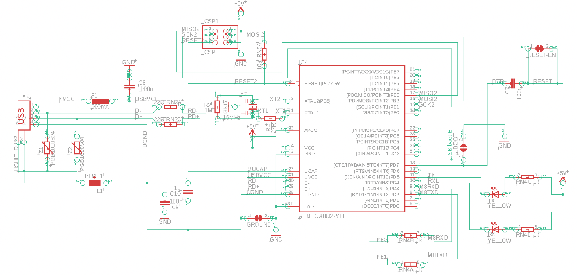
This figure shows a small section of the Arduino
MEGA 2560 reference design schematic diagram.
Modern PCB design software can translate the circuit diagram to a PCB layout, and these auto-generated layouts can be sufficient in many simple cases. However, most projects,
especially more involved ones, require manual adjustments or a fully custom design. During this step, engineers place the components from the schematic on a 2D plane that represents the PCB. They then draw traces between the electrically connected pads of the electronic devices in a process generally referred to as routing. While the schematic diagram defines the connections in the circuit, the PCB design dictates how the parts will be mounted on the resulting PCB and where the traces between them run. During this step, experienced engineers can leverage several powerful methods, such as managing power distribution and signal integrity considerations, to enhance the quality of their designs. Further, they can also add test points and create their designs with testability in mind, especially during the early prototyping phases of a project.
After they have laid out and connected all the components, designers can add silkscreen markers to the finished layout to document their design and help with assembly, troubleshooting, and testing. These markers commonly include component names, orientation guides for polarized parts, electrical characteristics (e.g., the capacitance of a part), or meta-information, such as the design revision. They can also change the PCB’s shape and size and add mounting holes, separation gaps, and similar structures.
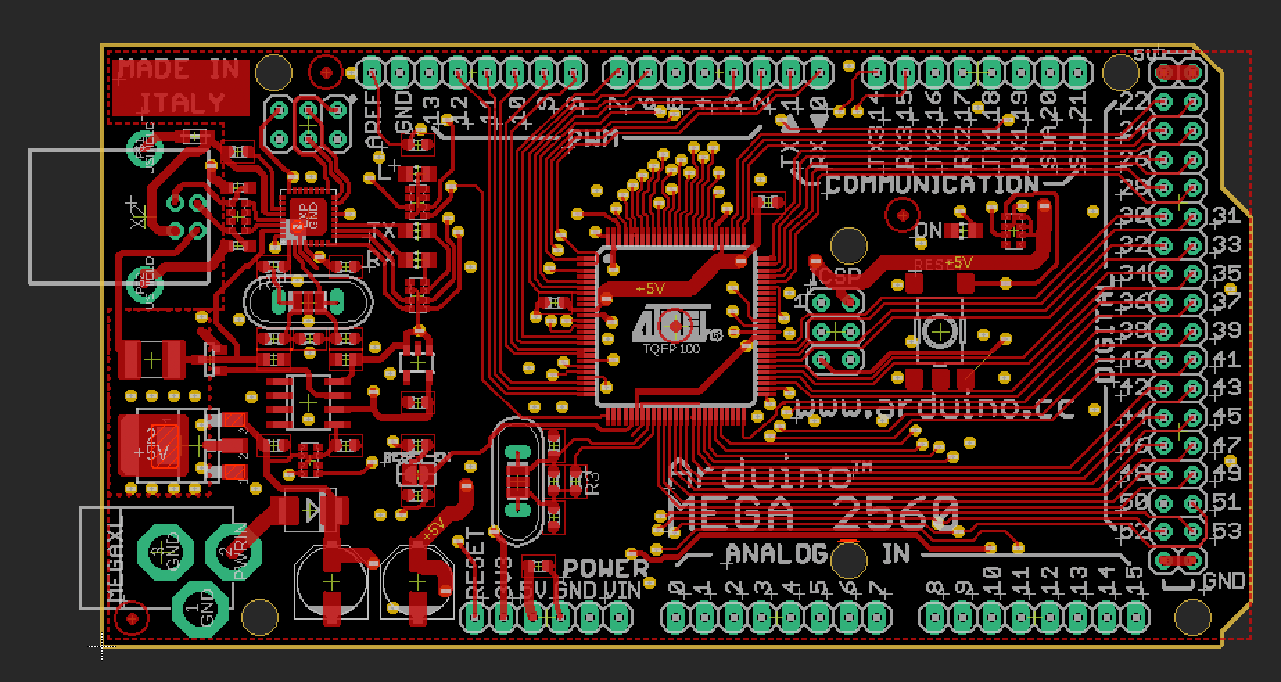
This screenshot shows the top layer of the finished reference PCB design.
At this stage of the design project, many modern design suites also allow for the generation of a 3D-rendered preview of the resulting board and the components to help visualize how the project will look. These previews can often also be exported to CAD software for designing enclosures and simulating thermal properties.
Exporting and Submitting a Design
Engineers must export the finished PCB layout according to the manufacturer’s design and file format specifications. During this step, they can leverage the power of automated design rule checks (DRCs) and electrical rule checks, which are vital processes that ensure the design’s integrity, functionality, and manufacturability.
More specifically, the DRC is a set of rules or constraints applied during the PCB layout phase to ensure that the design meets specific criteria defined by the manufacturer, industry standards, or project-specific requirements. The DRC could include a rule that ensures that all traces have a certain minimum width and sufficient clearance. In contrast, the ERC checks for errors in the logical connectivity of components, thereby maintaining the accuracy of the schematic representation and ensuring that the intended electrical connections are reflected in the design.
The PCB Manufacturing Process
Once exported and submitted, the manufacturer starts fabricating the PCBs, which involves a series of steps that require high accuracy and stringent quality control to ensure consistently good results. Generally, manufacturers don’t etch a single board at a time. Instead, they organize multiple designs or copies of a design in larger groups in a process called panelization to maximize efficiency and reduce cost and production waste.
After panelization, manufacturing proceeds with substrate and material preparation according to the customer’s specifications. When making rigid PCBs, a typical base substrate is FR-4, a glass-reinforced epoxy laminate that exhibits excellent electrical insulating properties, mechanical strength, and flame retardant properties. This base material is then coated with a conductive layer, typically a very thin sheet of copper foil.
This copper surface is treated with a light-sensitive layer that hardens when exposed to UV light. During this step, the manufacturer creates a photomask representing the panelized designs. During development, exposure to UV radiation leads to hardening of the photoresist layer. The photomask overlay shields the regions of the copper that should not be removed during etching, as the unexposed areas don’t harden and can then be washed away by a chemical solution.
Subsequently, a chemical agent reacts with the unshielded copper, removing the unwanted conductive material and only leaving behind the desired traces and areas as defined in the PCB layout. Lastly, a chemical washing step removes the hardened areas of the photoresist from the panel, leaving behind only the final copper areas and traces.
When producing designs with more than two layers, manufacturers apply chemical treatment to the copper layers of the inner base PCB for better bonding. They then add thin sheets of a different base material, called prepreg, and stack the layers, sandwiching the base in the middle. The outer sides of the prepreg also contain copper layers and alignment holes in all layers ensure correct alignment. After stacking, the layers get fused using high pressure and heat, forming a single solid stack with four copper layers in the final PCB. Precise pressure and temperature control ensures the correct bonding of layers and prevents delamination during the product’s lifetime. Automated optical checks ensure that the inner copper layers are flawless.
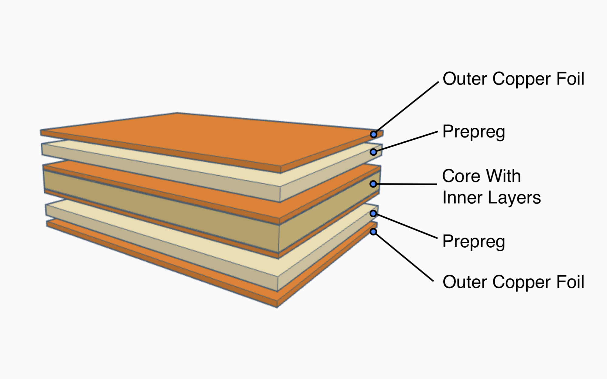
This image portrays an exploded view of a four-layer PCB before pressing and without depicting the traces already etched in the copper layers.
Next, CNC machines drill holes and cut slots as defined by the engineer. Additional electroplating can increase the thickness of the copper traces. Then, factories usually apply the solder mask, often giving PCBs their characteristic green color. However, engineers can typically choose from different colors and surface finish options. Aside from the visual aspects, the solder mask inhibits corrosion and facilitates efficient assembly by preventing the solder from unintentionally sticking to traces and bridging pads. The silkscreen is then printed on the solder mask before applying an additional optional surface finish, such as HASL or ENIG, to protect the copper solder pads and enable fast assembly.
Finally, the manufacturer separates the individual designs on the large panel before performing electrical testing, automated optical inspections, and other quality control measures. The finished PCBs are then packaged and shipped to customers.
Summary
Engineers can begin by drawing a schematic diagram that defines the electrical characteristics of the circuit. Applying various techniques and a forward-thinking approach can significantly streamline the subsequent design steps. Next, experienced engineers strategically place components and draw traces between them to create the PCB layout. Automated Design Rule Checks (DRCs) and Electrical Rule Checks (ERCs) ensure design integrity.
From the manufacturer’s perspective, fabrication begins with substrate and material preparation. Rigid PCBs commonly use FR-4, coated with a thin copper layer. Design rule adherence is verified, and panelization organizes designs efficiently. A photomask representing panelized designs is created, and after exposure and chemical washing, unwanted copper is etched away. For multi-layered designs, layers are aligned, bonded, and drilled. Solder mask application follows, inhibiting corrosion and aiding assembly. Silkscreen markers are added, and optional surface finishes are applied.
Finally, manufacturers separate individual designs from the panel before conducting electrical testing, automated inspections, and other quality control measures. Finished PCBs are then packaged and shipped.
