


Ground and power planes are large conductive areas in a PCB design that serve diverse purposes. Ground planes provide a common reference point for electrical signals and serve as return paths for currents. Power planes carry power supply voltages to various components on the board to help distribute power evenly across the entire PCB, thereby reducing voltage drops and ensuring a steady supply. While supply planes offer numerous benefits, they also come with the added need for careful planning of current return paths to prevent signal degradation, especially in mixed-signal designs.
Significance of Power and Ground Planes
Ground planes help reduce noise and EMI by providing a low-impedance path for return currents, thereby improving and maintaining signal integrity. Combined with power planes, they also enhance power delivery and help prevent brown-out issues in applications that exhibit short, sudden spikes in their power requirements. The added solid conductive material also helps spread the heat generated by components on the PCB, thus facilitating improved thermal management without additional cost. For designers, GND and power planes offer simplified routing and higher-density designs by removing the need to route GND and power traces manually.
Conversely, reference and power planes may also offer some challenges due to the physics involved in electronics. Any two adjacent layers in a PCB naturally form a capacitor due to the proximity of conductive elements and the dielectric material between them. This process includes the signal trace layers and supply planes, which can cause problems when not accounted for in the PCB design.
Multi-Layer PCB Return Current Paths
In purely digital designs with low signal rise times in the order of a few nanoseconds, the return current path tends to follow the trace that carries the signal closely. The induced current in the nearest GND plane is spread out in a shape that resembles a narrow Gaussian distribution. However, the return current path in analog designs may not directly follow the trace. Instead, the return current may span a relatively broad area around the trace that transmits the analog signal. In these cases, the spread area tends to be larger the lower the switching frequency of the analog signal.
When traces are routed directly above solid reference planes, the return current typically has a direct low-impedance path to that plane. In other cases though, the return current path continues through the entire layer stack-up until it reaches a suitable reference plane. When not accounted for and carefully planned, these return current paths can become very long and ultimately resemble indirect routing between the signal layers without a suitable reference plane in between. This induced current can result in cross-talk and signal degradation between analog and digital sections of a mixed-signal PCB design.
Mitigating Return Current Path Problems
One way to navigate this problem is by placing all components that induce return currents on the side closer to the GND plane to optimize return paths. Alternatively, additional decoupling capacitors between the power and GND planes can mitigate EMI problems by providing a low-impedance path for the return current to GND.
Layer stack-up optimization might be suitable for designers to avoid introducing new or relying on existing decoupling capacitors. For example, in a four-layer PCB design the top layer may be used for signal and power lines, and the bottom layer could contain signal traces exclusively. The two inner layers are available for reference planes. Then, both outer signal layers have a direct low-impedance path to one of the inner GND planes. More complex designs may require the introduction of more than four layers so that signal traces can always be routed directly above a suitable reference plane.
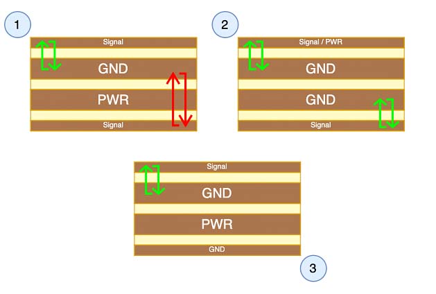
This figure illustrates three possible ways of arranging the layers in a four-layer PCB design.
Very low-impedance PDNs can be achieved using the two bottom layers as GND and power planes, the top layer for signals, and an additional GND plane directly underneath the signal plane. This approach can benefit designs with high current draws or fast-switching components.
Ground Plane Design in Mixed-Signal Design
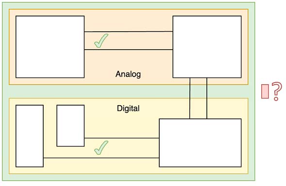
In mixed-signal PCB design, the ultimate goal of ground plane design is to isolate and separate mixed-signal areas as much as possible to prevent interference. If that’s not viable, designers should ensure that digital circuitry does not induce currents in analog sections of the PCB, as analog circuits are generally more predisposed to noise.
Physically separating the GND plane into multiple smaller ones is generally not recommended in modern designs to prevent problems caused by undefined return current paths between planes. Instead, complete separation should only be done when physically isolated GND signals are required for regulatory or physical reasons, such as in safety-critical applications, isolated power converters, or high-power applications.
The return current paths directly above the respective regions are well defined. However, the exact behavior in the gap between the isolated reference planes is difficult to estimate.
In mixed-signal A/D circuits, multiple ground planes may provide distinct references for the different signal classes. In those cases, however, designers typically want to connect the GND nets at a single point using a net tie. Therefore, the main goal is not physical separation but preventing digital noise from influencing more susceptible analog subcircuits on the PCB.
Considerations for Designing Separated Ground Planes
If physically separated AGND and DGND regions are required or wanted, designers must route digital signals only above a suitable digital reference plane. Similarly, analog traces must be situated above an analog GND plane to prevent EMI problems and signal crosstalk between the two regions.
If a net tie is wanted, it should be placed so that it doesn’t allow any return currents from one type of signal to make it over to a different reference plane. Total separation is generally easier to manage when simultaneously working with low-frequency analog and digital signals. A net tie may be more appropriate in mixed designs with high-frequency analog subcircuits.
In the case of isolated power converters, the primary and secondary GND nets should be connected by different means — for example, using a very high-value safety capacitor to allow noise from the output side to return to the input side through the capacitor, while maintaining an isolated barrier.
The Role of Stitching Vias and Their Effect on Traces
Via stitching is a technique that utilizes vias to tie together copper planes on different layers of a PCB. The method can help maintain short, low-impedance current return paths and create areas with low electromagnetic noise, as wanted in RF designs.
However, considering the potential impact of vias on nearby traces and planes is vital. Vias can introduce impedance discontinuities, reflections, and crosstalk, especially at high frequencies. In addition, vias can create gaps in solid reference planes, thus disturbing the current return paths of nearby traces. Therefore, careful placement and routing are necessary to mitigate these effects and ensure optimal PCB power distribution network performance.
The Bottom Line
Supply planes can help reduce noise and EMI and maintain signal integrity. However, they present additional challenges due to the physics involved in electronics. Designers must carefully consider and plan return current paths and their effects on nearby components and conductive layers, especially in mixed-signal designs.
Several methods can help mitigate the problems. One of the most common approaches is layer stack-up optimization, in which designers change the arrangement of layers in a multi-layer design to move signal layers above reference planes. Doing so ensures short, low-impedance return current paths to GND. Carefully placed decoupling capacitors can have a similar effect.
In mixed-signal designs, one way to overcome signal degradation is to spread out analog and digital components with very low frequencies as much as possible. Utilizing separate ground planes is generally only advised if physical separation is wanted or required — for example, due to safety regulations. Instead, designers should employ other means like a single net tie or safety capacitors. Via fences can also help create low-noise areas in mixed-signal PCB designs.
