


Advanced Circuits’ PCB Artist™ is a free and completely unrestricted printed circuit board design software that allows users the ability to create up to 28 layer boards with its Multipage Schematics, Controlled Autorouter, and components library of over 500k parts. The complete version of the software can be downloaded from the Advanced Circuits’ website or from CNet’s Downloads.com where it is listed as the most popular PCB design software with over 250,000 downloads.
In this two part post, we will discuss the basics of creating a printed circuit board design using PCB Artist™ in the following sequence:
Circuit Board Design Part 1
- PCB Artist™ Design Toolbar and Menu Introduction
- PCB Schematic Design
- Adding PCB Components
Circuit Board Design Part 2
- Converting the Schematic to PCB Layout
- Design Rule Check
- In-App PCB Ordering
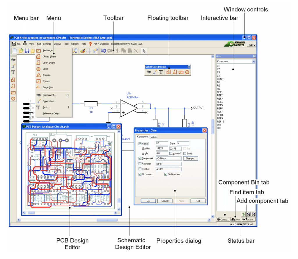
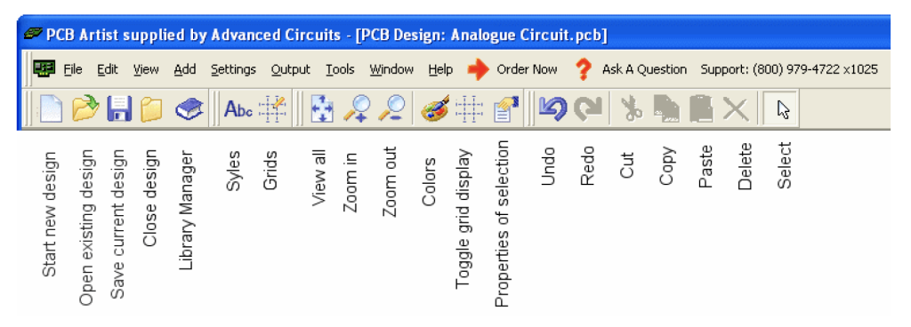
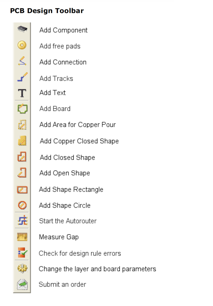
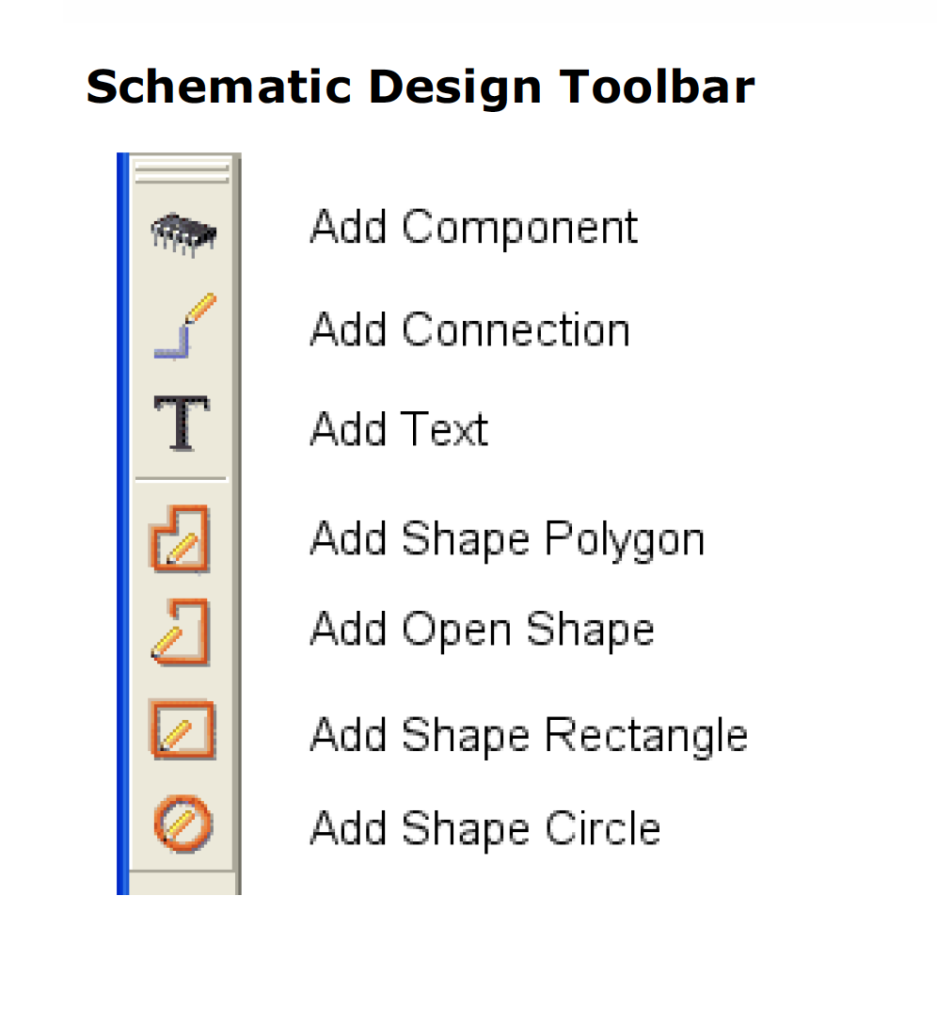
PCB Artist Design Toolbars and Menus
PCB Artist™’s professional-grade features make it easy to design your first or your next printed circuit board with intuitive toolbars and menus. Below, we identify the design software’s most common tools and menus:
Start PCB Design in Layout Mode or Schematic Design Mode
PCB Artist allows the users to begin the PCB design process in PCB layout mode or in schematic design mode. In this post, we will start our printed circuit board design process in schematic design mode. First, the user will need to start the PCB Artist™ software and click on File>New or hit Ctrl+N once the software is up and running. Then, select the New Schematic Design option and click on Use Template to get started quicker in the New Design Window.
Once you clock Ok PCB Artist™ will open a blank window with the Schematic Design Toolbar prominently displayed on the left hand side of the screen.
Let’s begin by adding components to the PCB Artist™’s Schematic Design area which for now should look like a blank canvas. When the Schematic Design option was selected, PCB Artist™’s Interaction Bar should be displayed; Select the Add Component browser at the bottom of the Interaction Bar and select the Component Library from the All Libraries list. When the appropriate Component Library has been selected, continue to find the component symbols needed for your Schematic and click the Add Component button.
Before connecting the components, you can move the components you have placed by simply clicking and drawing with your mouse. Components can be rotated during move by clicking the “R” key. A single click of the “R” key will rotate the component by 90 degrees. Click “R” more than once to rotate it by another 90 degrees and so on. Note that the components can also be moved after they have been connected.
After you have moved the components to the necessary location per your design requirements, the next step is to connect them. Connections are added to the Schematic design to make connectivity between electrical pins. When translated to the PCB design, these connections give you the circuit board design’s Net List.
An easy way to connect the components is to add connections by dragging off pins. Each click of the mouse after dragging will create a corner to the connection and moving the mouse to another electrical pin will allow you to finish the connection.
Once this is done, Power and Ground symbols can be added. Power and ground symbols are used in the Schematic to indicate a connection to a power source. These symbols are required for aesthetic purposes and are not translated to the PCB (because they do not have PCB footprints associated with them).
Now that your PCB design Schematic is finished, you are ready to move on to the next stage which is to convert the Schematic design into the actual PCB layout. As we mentioned before, it is not necessary to begin your PCB layout process in the Schematic mode since PCB Artist™ allows you to begin the PCB design in PCB layout mode as well. In the second part to this blog post, we will convert the Schematic to the PCB layout environment of PCB Artist™.
